Tenstorrent Wormhole Series Part 1: Physicalities
A company called Tenstorrent design and sell PCIe cards for AI acceleration. At the time of writing, they've recently started shipping their Wormhole n150s and Wormhole n300s cards. After taking the shell and the heatsinks off, the underlying circuit board looks like:
| Wormhole n150s | Wormhole n300s |
|---|---|
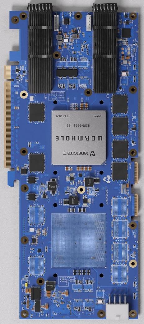 | 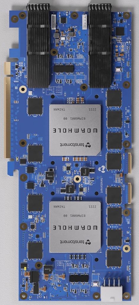 |
At the top of the board, there are two QSFP-DD cages for ethernet, which are intended for direct-attach cables between cards, as shown here. The left edge has a PCIe 4.0 x16 connector, which is connected to the immediately adjacent Wormhole ASIC. The Wormhole ASIC is surrounded by six GDDR6 chips (two on the left, four on the right), with each GDDR6 chip containing two 1GB banks, for a total of 12GB GDDR6 connected to the Wormhole ASIC. The right edge has two of what Tenstorrent call a Warp 100 Bridge connector, which seems to be a proprietary 100Gb ethernet connector. After this, the two boards diverge: the n300s card has another Wormhole ASIC with another 12GB of GDDR6 attached, whereas the n150s card has a bunch of empty space. The 2nd Wormhole ASIC on the n300s card is not connected to PCIe. Instead, on the n300s card, there are internal ethernet links between the two ASICs. Accordingly, for the host to communicate with the 2nd ASIC, it needs to use PCIe to communicate with the 1st ASIC, and ask the 1st ASIC to use its internal ethernet to communicate with the 2nd ASIC's internal ethernet.
The Wormhole ASIC itself is described as a 10 by 12 grid of tiles, arranged as:

There are a few different types of tile:
| Kind | Count | Contents (per tile) |
|---|---|---|
| ARC | 1 | 1x Argonaut RISC Core (also connected to PCIe) |
| D | 6 x 3 | Bridge to 2x 1GB GDDR6 (shared by three tiles) |
| E | 16 | 1x Baby RISC-V CPU (E variant) 256K SRAM Bridge to 100Gb ethernet (if connected) |
| PCIe | 1 | Bridge to host over PCIe |
| T | 80 (not all usable) | 5x Baby RISC-V CPU (B/T/T/T/NC variants) 1.5MB SRAM 1x Matrix unit (2048 multipliers, each 5b x 7b) 1x Vector/SIMD unit (32 lanes, each 32b wide) |
Each E tile can manage 100Gb ethernet (that is, simultaneous transmit at 100Gb/s and receive at 100Gb/s). On the n300s card, E8 of the 1st ASIC is connected to E0 of the 2nd ASIC, and E9 of the 1st ASIC is connected to E1 of the 2nd ASIC. Other tiles are connected to the QSFP-DD cages and to the Warp 100 Bridge connectors (possibly two E tiles on the 2nd ASIC route to the Warp, and four E tiles on the 1st ASIC route to the QSFP-DD cages). There's not enough I/O on the n150s/n300s boards to allow all the E tiles of a single ASIC to be connected, let alone all the E tiles of two ASICs to be connected; you'd need to buy a Galaxy Server to find a form factor with enough I/O to saturate all the E tiles.
Each tile has four outbound connections to its (north/east/south/west) neighbours, along with four corresponding inbound connections from its neighbours, with each connection being 32 bytes wide (apparently upgraded to 64 bytes wide in the next-generation Blackhole ASIC). The combination of the east-bound and south-bound channels are called NoC (Network on Chip) #0, whilst the combination of the west-bound and north-bound channels are called NoC #1. Going eastward from the eastmost edge lands you on the westmost edge (e.g. going east from the T at (9, 3) gets you to PCIe at (0, 3)). A similar thing is true on the other three edges: they are each connected to the edge on the opposite side. Taking the eastbound connections in row 3 as an example, we have:

It looks like the path between most neighbours is short, but then the wraparound path is extremely long. This would make both software and hardware designers unhappy, so the physical reality interleaves tiles to equalize the distances:

A similar interleaving is done to the columns, meaning that the actual physical locations of the various tiles within the grid is closer to:

The various tile-to-tile connections aren't shown on the above, as it would be a horrible mess of overlapping and dodging lines. It does however match the circuit board photos: the DRAM tiles are on the left and right edges, and tiles routing to the same DRAM chip are adjacent (e.g. the three D5 tiles are physically adjacent, even though their logical Y coordinates are 3, 8, 4). The ethernet tiles also end up on the physical edges, which makes sense. Thankfully, software mostly doesn't need to worry about this interleaving (except for HARVESTING_NOC_LOCATIONS, which you'll note are the Y coordinates of an interleaved column of T tiles), and can instead stick to the original logical view:
That said, there's one physical reality that software can't escape: manufacturing defects. You could imagine TSMC having a master template Wormhole ASIC and then photocopying it thousands of times to create the ASICs that actually ship to customers. As with actual photocopying, the photocopies are slightly lower quality than the original. Sometimes the defects are benign, but other times the defects completely ruin the piece of logic or storage that they occur within. Throwing away an entire ASIC because of a single defect would not be viable, so there are various strategies to deal with the defects. One such employed strategy is to disable (or "harvest") an entire row of T tiles if there is a defect in any of the T tiles in that row, effectively pretending that all the T tiles in that row are empty tiles (in the same way that e.g. (0, 2) is empty but still participates in the connection grid). An ASIC with one row of disabled T tiles can be used in an n150s board, which is why the n150s is reported as having 72 T tiles despite the ASIC having 80. Similarly, an ASIC with two rows of disabled T tiles can be used in an n300s board, which is why the n300s is reported as having 64 T tiles per ASIC despite there originally being 80. If the photocopying process had fewer defects than planned for, then one (n150s) or two (n300s) rows of T tiles are disabled regardless, for consistency (of what customers receive, of power usage, etc.). The non-T tiles within a disabled row are kept, though they become slightly harder to address. In particular, some workloads want to really minimise latency to DRAM, so want to run on a T tile immediately adjacent to a D tile. Some rows have 2 D tiles and thus four T tiles immediately adjacent to a D tile, whereas other rows have only 1 D tile and thus only two T tiles immediately adjacent to a D tile. Whilst each PCIe card will have the same number of usable T tiles (72 for n150s, 64 x 2 for n300s), the number of usable T tiles immediately adjacent to a D tile will vary randomly from card to card depending on which rows were disabled.
That wraps up part 1. If you're reading along, part 2 is next.